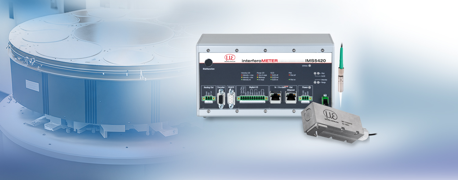
Vitljusinterferometer för högexakta inline-tjockleksmätningar av wafers
IMS5420 är en högpresterande vitljusinterferometer för beröringsfri tjockleksmätning av monokristallina kiselwafers. Kontrollern har en bredbandig luminiscensdiod (SLED) med ett våglängdsområde på 1 100 nm. Den möjliggör tjockleksmätning av odopade, dopade och högdopade Si-wafers med endast ett mätsystem och med en signalstabilitet på mindre än 1 nm. Beroende på användningsområdet finns sensorer med stort basavstånd och sensorer med friblåsningsanordning tillgängliga.
Detaljer
- Nanometer-accurate thickness measurement of undoped, doped and highly doped wafers
- Multi-peak: acquisition of up to 5 layers with an SI thickness of 0.05 up to 1.05 mm
- High resolution in z-axis of 1 nm
- Measuring rate up to 6 kHz for fast measurements
- Ethernet / EtherCAT / RS422 / PROFINET / EtherNet/IP
- Easy parameterization via web interface
Precise wafer thickness measurement
Due to the optical transparency of silicon wafers in the wavelength range of 1,100 nm, the IMS5420 interferometers can precisely detect the thickness. In this wavelength range, both undoped silicon and doped wafers provide sufficient transparency. Therefore, wafer thicknesses up to 1.05 mm can be detected. The measurable thickness of the air gap is even up to 4 mm.
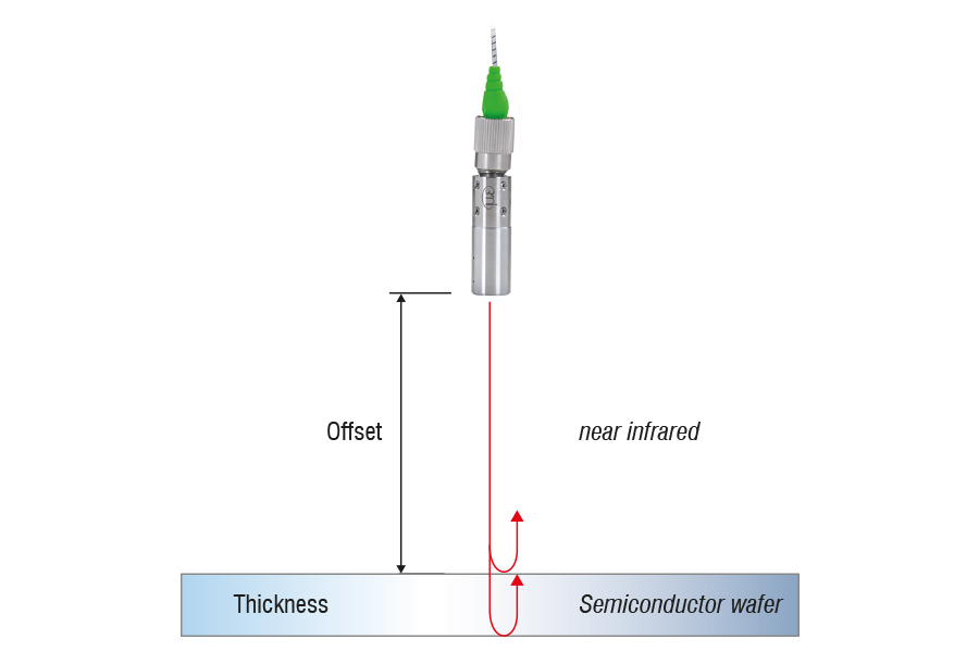
IMS5420 interferometern möjliggör tjockleksmätning av odopade, dopade och högdopade kiselwafers och ger därmed ett mycket brett spektrum av applikationer. Systemet för mätning av wafertjocklek är som gjort för mätning av monokristallina kiselwafers med en geometrisk tjocklek på 500 till 1050 µm och en dopning på upp till 6 m Ω cm. Trots att transparensen minskar med ökande dopning kan tjocklekar på upp till 0,8 mm fortfarande mätas även på högdopade wafers.
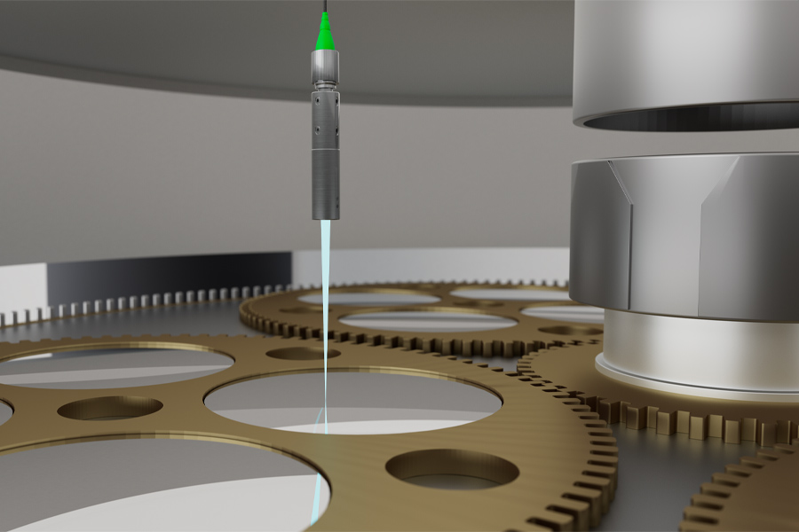
Exakt tjockleksmätning under läppningen
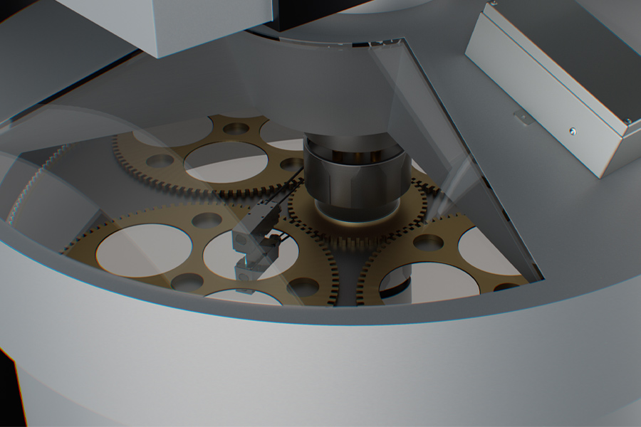
I wafertillverkningen sågas först en kristallin kiselenkristall i ungefär 1 mm tunna skivor. I den efterföljande slipnings- och läppningsprocessen får wafrarna den slutliga önskade tjockleken och samtidigt uppnås en hög ytkvalitet. För en stabil och reproducerbar processtyrning integreras interferoMETER för inline-tjockleksmätning direkt i läppnings- och slipmaskiner. De registrerade tjockleksvärdena stödjer både maskinregleringen och kvalitetssäkringen av varje enskild wafer.
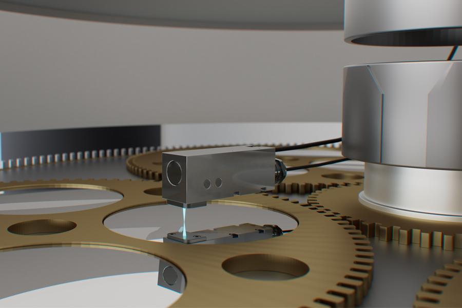
Kompakt sensor IMP-NIR-TH24
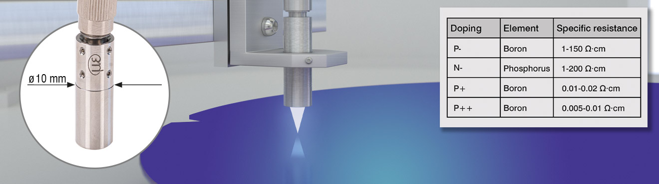
Med den slanka diametern på bara 10 mm och det samtidigt stora arbetsavståndet på 24 mm är IMP-NIR-TH24 perfekt lämpad för att i efterhand monteras in i existerande anläggningar. Kombinerat med den justerbara monteringsadaptern (JMA) förenklas integreringen avsevärt eftersom det går att kompensera mindre monteringsavvikelser eller lutande lägen. På förfrågan kan både sensorn och ljusledare fås som UHV-utförande.
NYHET: robust sensor IMP-NIR-TH3/90/IP68
Med IMP-NIR-TH3/90/IP68 utökas portföljen med sensorer med en kraftfull sensor för särskilt anspråksfulla monteringssituationer och tuffa omgivningsförhållanden. Givaren imponerar med en 90°-strålgång och ett litet arbetsavstånd på endast 3 mm – perfekt för mycket trånga monteringssituationer. Tack vare det robusta höljet (IP68) är sensorn dessutom lämpad för användning i särskilt anspråksfulla tillämpningar, som exempelvis vid slurry-slipning. Den integrerade friblåsningsanordningen håller kontinuerligt strålgången fri från smuts och möjliggör därmed konstant mätnoggrannhet – även i mycket kontaminerade miljöer.
Ett stort antal modeller för anspråksfulla mätuppgifter
| Modell | Arbetsavstånd/mätområde | Linjäritet | Antal mätbara skikt | Användningsområden |
|---|---|---|---|---|
| IMS5420-TH | Arbetsavstånd IMP-NIR-TH24 ca 24 mm (21 – 27 mm) | IMP-NIR-TH3/90/IP68 ca 3 mm (1 – 6 mm) / 0,05 – 1,05 mm (med kisel/n=3,82), 0,2 – 4 mm (med luft, n=1) |
< ±100 nm | 1 skikt | Inline-tjockleksmätning, t.ex. efter slipning eller polering. |
| IMS5420MP | < ±100 nm med ett skikt < ±200 nm för ytterligare skikt |
upp till 5 skikt | Inline-tjockleksmätning t.ex. vid kvalitetskontroll av skikttjocklek efter beläggningen. | |
| IMS5420/IP67 | Arbetsavstånd IMP-NIR-TH24 ca. 24 mm (21 – 27 mm) / 0,05 – 1,05 mm (med kisel/n=3,82), 0,2 – 4 mm (med luft, n=1) |
< ±100 nm | 1 skikt | Industriell Inline-tjockleksmätning under läppning och slipning. |
| IMS5420/IP67MP-TH | < ±100 nm med ett skikt < ±200 nm för ytterligare skikt |
upp till 5 skikt | Industriell inline-tjockleks- och flerskiktsmätning under läppning och slipning. |
Moderna gränssnitt för integration i maskiner och system
Styrenheten erbjuder integrerade gränssnitt som Ethernet, EtherCAT och RS422 samt ytterligare pulsgivaranslutningar, analoga utgångar, synkroniseringsingångar och digitala I/O. Detta gör att interferometern kan integreras i alla styrsystem och produktionsprogram.